Table Of Content
An ideally implemented code summarization can insert inline documentation into code blocks or generate separate documentation. With its help, the maintainability and documentation of the code can be significantly improved. The verification challenges that are addressable by ML and the techniques and algorithms that show promise.
The Importance of Pump Condition Monitoring in Semiconductor Manufacturing
This translates into a need for advanced EDA solutions that can manage the complexities of these designs. Leading EDA companies are offering industry-specific solutions, further bolstering the market's growth potential. Extensive ML studies have demonstrated that they can do better than random test generation.
Learn About AWS
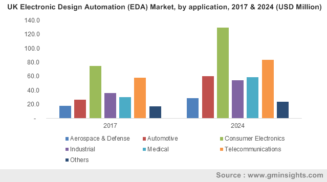
Electronic Design Automation Market to grow by USD 7.50 billion from 2022 to 2027, Growth Driven by the growing ... - Yahoo Finance
Electronic Design Automation Market to grow by USD 7.50 billion from 2022 to 2027, Growth Driven by the growing ....
Posted: Mon, 18 Sep 2023 07:00:00 GMT [source]
Want to learn how Helix Core and Helix IPLM can support your EDA tools and enhance your semiconductor planning and design process? Connect with one of our experts today to ask questions, schedule a demo, and learn more about getting started with these solutions. As the semiconductor industry consolidates and design teams collaborate across multiple geographies, securing all the IP blocks that go into a design becomes a challenge.
How will it affect the American chip companies?
After the fab has finished designing semiconductor devices and manufacturing processes, it must use EDA tools to create PDKs, standard cell libraries, and IPs. Lithography calculations and yield enhancement during the wafer manufacturing process are also tasks that must be completed using EDA software tools. Device model extraction tools, process and device simulation (TCAD), PDK development and verification, computational lithography, mask calibration, mask synthesis, and yield analysis are examples of wafer fabrication EDA tools. Since semiconductor design comes with complex challenges and high stakes – including strict regulations, tight time-to-market timelines, and an immense cost of error – teams need strong, trusted design tools.

Call for Nominations for Editor-in-Chief of the IEEE Embedded Systems Letters
Deficiencies in this area can cause the resultant chip to either not function or function at reduced capacity. Learn how Microsoft leverages Solido IP Validation to address IP quality issues early in the design process, saving time and money on potential (ECOs), improving overall IP quality in production and integration flows. In summary, we work with virtually every part of the EDA tool ecosystem to advance the delivery of the most impactful silicon chips in the industry today. Our teams experiment, share, and learn continuously to improve EDA workloads that are crucial for our business. Silicon based chips are the heart and soul of virtually every electronic device that improves human lives today.
Topics of ML in functional verification
Recent surveys indicate that functional verification is still the most time-consuming step in IC design, and functional and logic errors are still the most important cause of a respin. Any improvement in the speed of functional verification will significantly impact the quality and productivity of IC design. ML has been used in both formal and simulation-based verification for their acceleration. At the time of this writing, code summarization in IC design verification has not yet been reported in any literature.
Design and Test of Offset Quadrature Phase-Shift Keying Modulator with GF180MCU Open Source Process Design Kit
A gradient-based search on a trained Graph Neural Network (GNN) is used to generate tests for a predefined test target. The experiments on IBEX v1, v2, and TPU achieved 74%, 73%, and 90% accuracies at coverage prediction when trained with 50% cover points. Several additional experiments also confirm that the gradient search method employed is insensitive to the GNN architecture. A promising idea being discussed and experimented with is to use of ML to model and predict the behavior of a complex system.
IC Design Flow
It is reasonable to be optimistic that the success of other languages can be realized in IC design and verification, which has yet to be confirmed by the research community. In particular, recent progress with cross-language models might help transfer learned knowledge from other programming languages to IC design. However, in addition to the challenges general to ML on code summarization, the intrinsic temporal parallelism in IC design and verification code can present challenges uncommon in other programming languages. The rise of system-on-chip (SoC) designs in the late 1990s and early 2000s marked a pivotal moment that led to EDA 3.0. This era witnessed the emergence of an IP development economy coupled with design reuse methodologies. EDA tools and standards were developed to support the design, verification, and validation of SoCs, enabling engineers to manage the escalating complexity of SoC-class designs.
What is China doing regarding EDA?
This presentation starts with the introduction of our FPGA-based SoC control system DUT and testbench, then discusses advantages and disadvantages of using Vivado and Questa Core for verification. Learn how Allegro MicroSystems leveraged AI-powered Solido Design Environment and Analog FastSPICE to accelerate PMIC verification, resulting in an overall 5X reduction in verification time. Learn how NVIDIA leveraged Solido Additive Learning technology to speedup standard cell library verification with Solido Design Environment while maintaining the same accuracy on verifying a new PDK revision. We use EDA to bring efficient, performant, and energy efficient solutions for every one of your use cases. We are enthusiastic champions of pervasive use of AI to advance EDA semiconductor solutions.
This phase of the industry was known as CAD/CAM (computer-aided design/computer-aided manufacturing). Simulation tools take a description of a proposed circuit and predict its behavior before is it implemented. This description is typically presented in a standard hardware description language such as Verilog or VHDL. Simulation tools model the behavior of circuit elements at various degrees of detail and perform various operations to predict the resultant behavior of the circuit. The level of detail required is dictated by the type of circuit being designed and its intended use.
Most recently he served as the Corporate Vice President of Research and Advanced Development at AMD. During his tenure at the company, he founded AMD Research where he oversaw the company’s worldwide research and advanced technology labs, university engagements, and external research contracting. Alan also led extreme-scale computing technology at AMD, where he drove the software and hardware engineering efforts to build the world’s fastest platforms for machine learning, industrial, and scientific applications. Electronics manufacturing organizations require increasing amounts of compute and storage for electronic design automation (EDA).
Another essential aspect of maintaining traceability is tracking who made each change and when these changes occurred, particularly as teams become more distributed. An IP lifecycle management solution like Helix IPLM records every change to your files, plus integrates with your existing electronic design automation infrastructure. While electronic design automation is necessary in the semiconductor industry, the increasing complexity of semiconductor design – along with global distribution of design centers and proliferation of tools used – pose new challenges. Dr. Gary L. Patton is corporate vice president and general manager of the Design Enablement group in Technology Development at Intel Corporation. Dr. Patton is a well-recognized industry leader in semiconductor technology R&D with over 30 years of semiconductor experience. He is a Fellow of the IEEE and recipient of the 2017 IEEE Frederik Philips Award for industry influence and leadership in the development of leading-edge microelectronics technology and collaborative research.
Electronic design automation (EDA), also referred to as electronic computer-aided design (ECAD),[1] is a category of software tools for designing electronic systems such as integrated circuits and printed circuit boards. The tools work together in a design flow that chip designers use to design and analyze entire semiconductor chips. Since a modern semiconductor chip can have billions of components, EDA tools are essential for their design; this article in particular describes EDA specifically with respect to integrated circuits (ICs). EDA serves as a bridge and connection linking the two links of integrated circuit design and manufacturing.
Speaking of sharing, for an in-depth discussion of many diverse types of EDA tools and how AMD performance improvements deliver tangible benefits to EDA customers, see the latest blog on EPYC CPUs excelling at EDA workloads from Raghu Nambiar. As a student passionate about electronic design and the semiconductor industry, I attend DAC to get a head start on my career. I am able to demonstrate my skills to design professionals and connect with mentors, recruiters, and future colleagues worldwide. I know that DAC can jumpstart careers by providing unparalleled networking and recruitment opportunities. However, due to the relative simplicity of the ML techniques adopted, they are not able to train ML models that can consider rich semantics in code or learn from historical bug fixes.


No comments:
Post a Comment